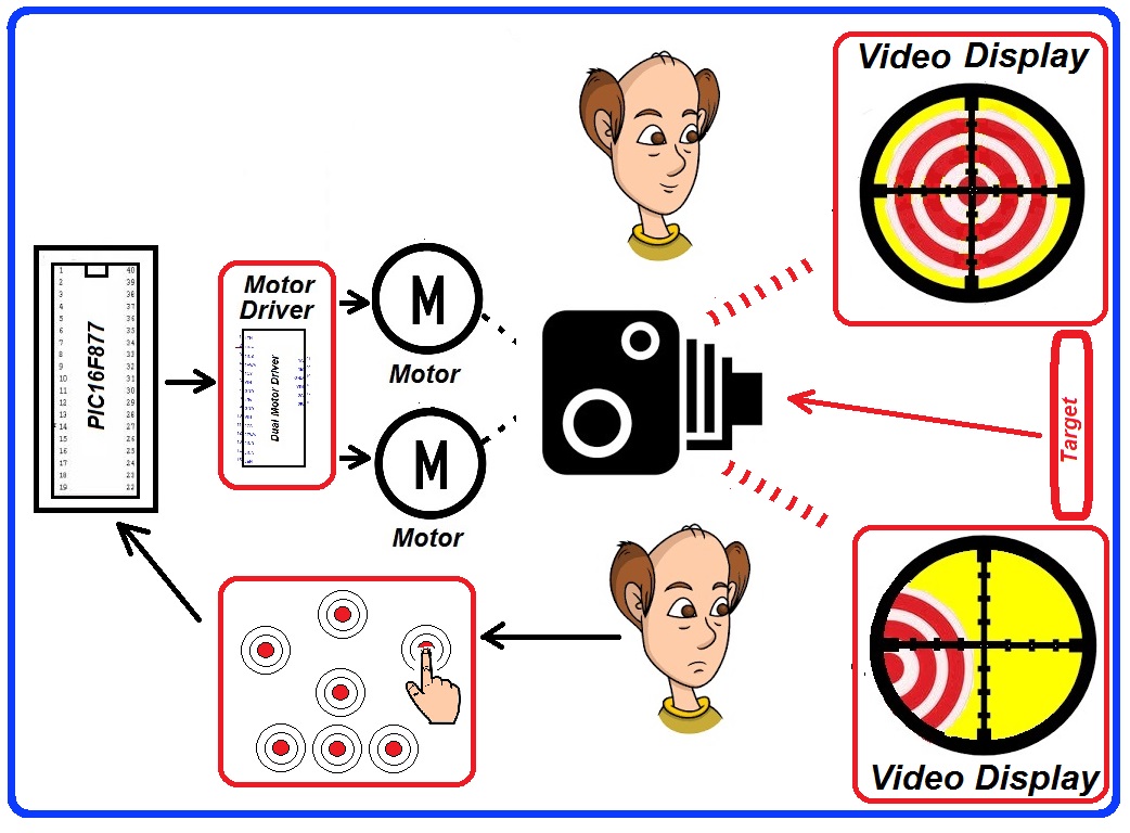
There are literally thousands of Microprocessor based Projects. Many Microprocessor based Projects are for the control functions in robotics. The selection for this post is special because there is a unique feedback loop involved in the robotics operation.
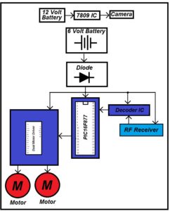
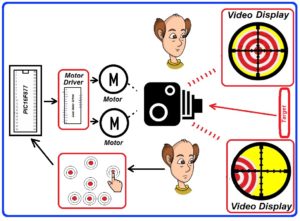
The camera (primary sensor) image goes to the display, then to the eyes of the user. The user presses the push buttons (secondary actuator) to correct the camera image. The push buttons feed the microprocessor, sending the appropriate signals to the motor driver, allowing the motors to move the camera’s position, correcting the camera image until the user is satisfied. completing the primary feedback loop in this Microprocessor based Project.
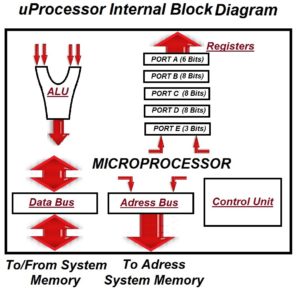
This is a very general block diagram of a microprocessor that could be used in Microprocessor based Projects.

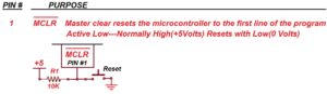
You must understand the meaning of the pin reference designations In order to program the device.
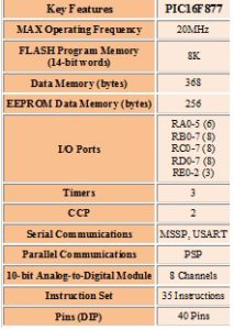
The Microprocessor based Projects major features of the PIC 16F877A include 368 bytes of RAM, 8K bytes of Flash, 256 bytes of EPROM, 3 timers and five I/O ports. It is based on reduced instruction set computing(RISC) architecture. The instruction set consists of thirty-five easy to understand instructions.
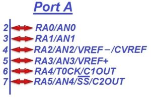
Pins 2 thru pin 7 make up port A. The six pins of port A are bidirectional Digital input/output pins. The data direction for each port pin is set with a corresponding bit of the TRISA register. (1=input &0=output). Pins with the AN designation can also be used as analog input pins but must be configured as input pins by the TRISA register and as Analog by the ANSEL register (Example: RA0 = AN0). A negative analog reference voltage can be assigned to pin 4. A positive analog reference voltage can be assigned to pin 5. Pin 6 can act as the clock input pin with an open drain output. Regarding Pin 7(RA5/SS/AN4), there is a synchronous serial port in the controller and this pin can provide the slave select for that port.
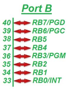
Pins 33 thru 40 comprise a bidirectional Port B. Individual pin data direction is controlled and maintained by the TRIS B Register. A one represents an input and a zero represents an output. Pins 36, 39, &40 are multiplexed allowing In-Circuit Debugging and Low-Voltage Programming. Pin 33 is multiplexed allowing an external interrupt.
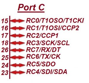
PORT C is an 8-bit wide, bidirectional PORT which is controlled and maintained by the TRIS C data direction register. Setting a TRIS C bit to a 1 will make the corresponding PORT C pin an input. Clearing a TRIS C bit to a 0 will make the corresponding PORT C pin an output. PORT C pins can be multiplexed to provide several additional peripheral functions.
Pin 16 (RC1/T1OSI/CCP2) can be the oscillator input for timer 1 or the capture 2 input/compare 2 output/ Pulse Width Modulation M 2 output pin.
PIN 17 (RC2/CCP1) can be the capture 1 input/ compare 1 output/ PWM 1 output
Pin 18 (RC3/SCK/SCL) can also be used as the synchronous serial clock i/o for both SPI or I2C modes.
Pin 23 (RC4/SDI/SDA) can be configured as the SPI data input pin.
Pin 24 (RC5/SDO) can be set up to be the SPI data output pin.
SPI (Serial Peripheral Interface) is a full-duplex synchronous serial communication interface used for short distance communications between different modules in a device or on a PCB.
PIN 25 (RC6/TX/CK) can be the synchronous clock or USART Asynchronous transmit pin.
PIN 26 (RC7/RX/DT) can be the synchronous data pin or the USART receive pin.
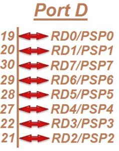
PORT D is an 8-bit bi-directional PORT. All pins in Port D include Schmitt Trigger input buffers, each pin is individually configurable as either input or output. The PORT D pins can be configured as an 8-bit wide microprocessor PORT by setting control bits, PSPMODE (TRISE<4>). In this mode, the input buffers are TTL.
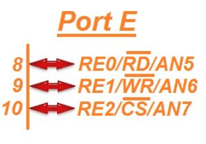
PIN 8 (RE0/RD/AN5) is a bidirectional input-output port. It can be configured as an analog input AN5 or as a parallel slave port it can act as a ‘read control’ active low pin.
PIN 9 (RE1/WR/AN6) is a bidirectional input-output port. It can be the analog input AN6 or as a parallel slave port, it can act as the active low ‘write control’ pin.
PIN 10 (RE2/CS/AN7) is a bidirectional input-output port. It can be the analog input AN7 or as a parallel slave port, it can act as a ‘control select’ which will also be a bidirectional input-output port. just like read and write control pins.
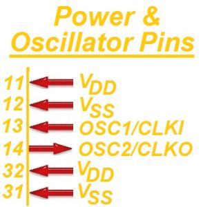
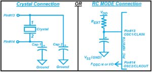
Pins eleven and thirty-two, both labeled VDD (drain supply voltage), should be connected to the positive five volt supply. Pins twelve and thirty-three, both labeled VSS (source supply voltage) should be connected to zero volts. Pin thirteen is the oscillator input or the external clock input. Pin fourteen is the oscillator output. An external clock signal is provided to the microcontroller by connecting a crystal resonator between pins thirteen and fourteen. Another option is to use the RC mode which outputs a frequency one fourth that of the of input.