Forming the PN Junction
Before explaining how the PN Junction works, a couple of concepts need to be clarified. When impurities are added to a semiconductor, the over all material is still neutral. The number of protons in the N or P material is still equal to the number of electrons in that material. What doping has done is to have introduced Free Electrons (negative charge carriers) or Holes (positive charge carriers) into the structure of the material. Containing the charge carriers makes it possible for the material to conduct current. Without the charge carriers the semiconductor material is an insulator.
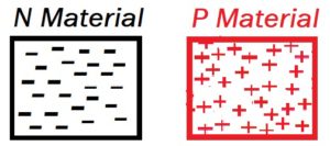
Another important concept is that "Like charges repel each other"and "opposite charges attract each other". By physically connecting P and N material a Junction is formed.
How the PN Junction works.
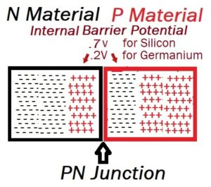
Once the two materials are joined to form a junction, the law of charges takes over causing the electrons in the proximity of the junction to cross over and fill holes on the other side. In doing so holes are created in the N material. An internal voltage is developed across the junction. Referred to as the barrier potential, it acts as a barrier to a current path through the material. The barrier is relatively thick in silicon junctions. The barrier potential in silicon junctions is approximately .7 volts. The barrier in germanium junctions is much thinner and the barrier potential is approximately .2 volts. These internal voltages can not be measured directly but they are present.
So now we have a PN junction with a barrier that's blocking current flow. By placing an external voltage across the junction we can control the barrier's thickness. Lets see what new terms are associated with the control of this barrier. There are two possibilities regarding the polarity of the external voltage. First: Positive connected to the P material and negative connected to the N material. Second: Positive connected to the N material and negative connected to the P material.
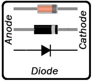
Crystal Junction Diode
